
Exosens markets
See all
Defense & Surveillance
Innovative and high-quality products that meet the needs of its customers in the fields of defense and surveillance.

Industrial Research & Control
Enhancing Industrial Research & Control: Test and evaluate without any damage

Lifescience & Environment
Imaging and detection solutions bring high image quality or low-level detection to enabling Life Science breakthroughs.

Nuclear
Nuclear instrumentation is essential to ensure safety, accuracy, and compliance in various nuclear-related activities.
Meet Exosens brands
See all


Discover our technologies
See all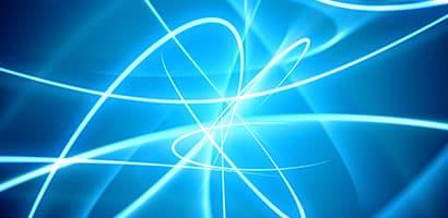
Ions & electrons detection technology
Discover technologies from both El-Mul and Photonis in the fields of high-performance ion, electron, and photon detection...

Visible technology
Explore the evolving world of visible technology technology that unlocks possibilities across various industries. Discover our expertise and solutions, shaping the future.

X-Ray technology
X-Radiation is a revolutionary scientific technology that has significantly and positively impacted various applications...
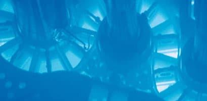
Gamma and Neutron technology
Gamma and Neutron detection technology is a cutting-edge field that significantly contributes to nuclear safety and research.

Ultra violet technology
Ultraviolet or UV, is a wavelength range below 400 nm or shorter than the visible wavelength. Explore Ultraviolet imaging technology across the full spectrum of UVA, UVB, and UVC
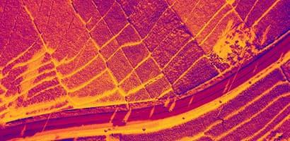
Infrared technology
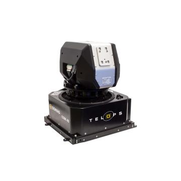
Combining the strengths of both Xenics and Telops technologies in the field of infrared imaging and camera systems lead to innovative and powerful solutions.

Microwave amplifiers
Microwave technology, particularly in the realm of RF amplification enhances the capabilities of electronic countermeasure systems...
What's new?
See all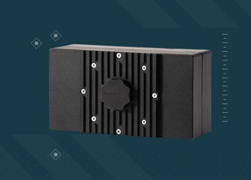
Apr 09th 2024
Exosens Adds Innovative Photon Counting System, LINCam


Feb 06th 2024
Occar renew their trust in Photonis' expertise
Photonis shall deliver 40,000 image intensifier tubes to boost military night vision in Germany and Belgium
Exosens products & services
Exosens is a global manufacturer of optoelectronics components used in the detection and amplification of ions, electrons and photons. We are focused on mission critical components aimed at highly demanding customers. We innovate and engineer quality components for integration into a variety of applications such as night vision optics, digital cameras, mass spectrometry, physics research, space exploration and many others.
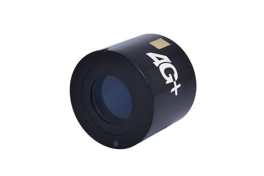
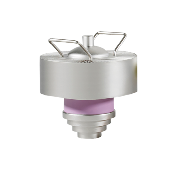
All productsImage intensifier tubes to amplify low light level images several thousand times, enabling clear vision in night and low light conditions.
 Discover
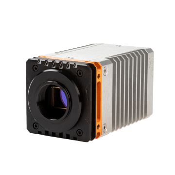
Exosens with its continuous innovation and commitment to offer advanced imaging solutions, proposes a diverse range of imaging technologies covering a large spectrum of light from below 300 nm Ultra Violet (UV) and up to 12,000 nm in the thermal spectral range Long Wave Infrared (LWIR).
 Discover
Exosens provides a wide range of innovative detection and imaging solutions globally, including detectors for photons, electrons, ions, neutrons, and X-rays.
 Discover
Neutron and gamma detectors are essential elements for the safety and control of nuclear reactors, fuel reprocessing plants, waste storage facilities, and research facilitiesies.
 Discover
The highest quality, hybrid power amplifiers, combining both vacuum electron and solid-state technologies.
 Discover
Telops offers a Methane Airborne Detection Service for the Oil and Gas Industry. Whether you are an oil and gas company, a potential service partner or a regulator society we are committed to addressing your inquiries and providing the necessary support.
 Discover
Our company
Leader in detection and imaging
Exosens is a high-tech company, accompanied by Groupe HLD since 2021, with more than 85 years of experience in the innovation, development, manufacture and sale of technologies in the field of particles and photo detection and imaging.
Today, it offers its customers detectors and detection solutions: its travelling wave tubes, advanced cameras, neutron & gamma detectors, instrument detectors and light intensifier tubes allow Exosens to respond to complex issues in environments extremely demanding by offering tailor-made solutions to its customers.
Thanks to its sustained and permanent investment, Exosens is internationally recognized as a major innovator in optoelectronics, with production and R&D carried out on 9 sites, in Europe and North America and over 1 500 employees.
85+ years of experience
1500+ Employees worldwide
130+ proven technology patents
50+ countries: 95% overseas revenues
6% of turnovers in R&D
4000m2 clean rooms